
Min. Order:100 Piece/Pieces
Transportation:Ocean,Land,Air,Express
Port:Shenzhen,Hongkong
$1-50 /Piece/Pieces
Model No.: Customized
Brand: Jinghui ceramics
Place Of Origin: China
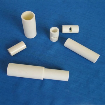
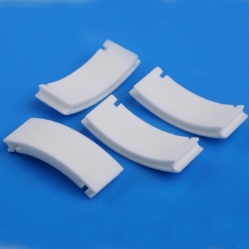
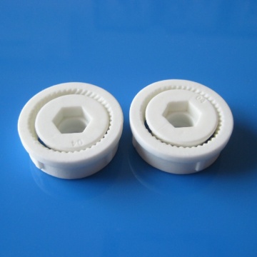
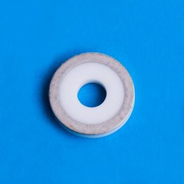
Types Of: High Frequency Ceramics, Dielectric Ceramics, Insulating Ceramics
Material: Alumina, Zirconium Oxide, Aluminum Nitride, Silicon Nitride, 95% Alumina, Aln Ceramics
Tolerance: Best To Be 0.01mm
Min. Wall Thickness: 0.3mm
Precision Process: Fine Grinding,Maching,Laser Cutting
Features: Excellent Insulation, Heat Dissipation
Application: Ceramic Circuit Board
Certificate: Iso9001:2015, Sgs
Color: White, Gray
Packaging: Export carton
Productivity: 100,000 sets/month
Transportation: Ocean,Land,Air,Express
Place of Origin: China
Supply Ability: 500,000 sets/month
Certificate: RoHS
HS Code: 8547100000
Port: Shenzhen,Hongkong
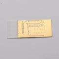
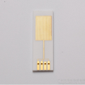
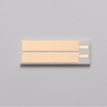
DBC (Direct Bonded Copper) is to directly bond pure copper (99.99%) to high-purity Alumina Ceramic or aluminum nitride ceramic substrate technology. The thickness of the copper foil can be controlled between 10~600um, and the circuit pattern can be directly bonded according to customer requirements.
DBC ceramic substrates offer excellent electrical insulation, thermal conductivity, super good heat dissipation. high temperature resistance, moisture resistance, corrosion resistance, stable size and dielectric properties. DBC ceramic substrate has been proven for ages as a proper solution for electrical insulation and thermal management of high power modules.
Our factory have been producing a broad range of DBC ceramic substrates, mainly including high purity alumina ceramic DBC susbstrate, aluminum nitirde DBC substrate, beryllium oxide DBC substrate and silicon nitride DBC substrates. These substrates are commonly used in high power LED, solar cell component, thermoelectric (Peltier) coolers and semiconductor refrigeration fields .
DBC Process Capability and Specification of DBC ceramic substrates
S/N Item Parameters 96% alumina (Al2O3), Aluminum nitride(AlN) ,Beryllium oxide (BeO) and Silicon nitride(Si3N4) 2 Processing type Direct Bonded Cooper (DBC) 3 Min. Distance 0.15mm 4 The thickness of conductor layer 0.075 ~ 600 um 5 Solder White, Black, Green 6 Surface treatment ENIPIG, Deposition 7 Typical thickness of raw substrate 0.30mm, 0.38mm, 0.50mm, 0.63mm and 0.80mm 8 Regular size 130mm x 140mm, 140mm x 190mm
1 Material type


High-density Hybrid Circuits, Microwave Power Devices, Power Semiconductor Devices, Power Electronic Devices, Optoelectronic Components,Semiconductor Refrigeration Products
Q1. Is it available to provide customize products?
A: We support customized DBC ceramic substrates with selection raw materials, designated thickness of DBC types.
Q2. How long can I expect to get the sample?
A: The samples could be ready in 2 weeks when all technical details are confirmed.
Q3. How long does the whole procedure being worked out?
A: It depends on the quantity level of order. In common case, the manufacturing time is about 25 working days after order confirmed.
Q4. How to ensure quality?
A: The reliability test, dimensional & cosmetic inspection will be performed with a certain sampling size every order.
Q5: What other products are you dealing with?
A: We focus on a variety of technical Ceramic Tubes, Industrial Ceramic Plate, Ceramic Seals besides DBC ceramic substrates.
Q6. Are you a factory or trading company?
A: We are a professional manufacturer. We are warmly welcome clients from worldwide to visit our factory and cooperate with us.