
Payment Type:T/T,Paypal,Western Union
Incoterm:FOB,CFR,CIF,EXW,FCA,CPT,CIP
Min. Order:100 Set/Sets
Transportation:Ocean,Land,Air
Port:Shenzhen Port,Hongkong Port
$5≥100Set/Sets
Model No.: Customized
Brand: Jinghui ceramics
Packaging: Export carton
Productivity: 100,000 sets/month
Transportation: Ocean,Land,Air
Place of Origin: China
Supply Ability: 500,000 sets/month
Certificate: RoHS
Port: Shenzhen Port,Hongkong Port
Payment Type: T/T,Paypal,Western Union
Incoterm: FOB,CFR,CIF,EXW,FCA,CPT,CIP
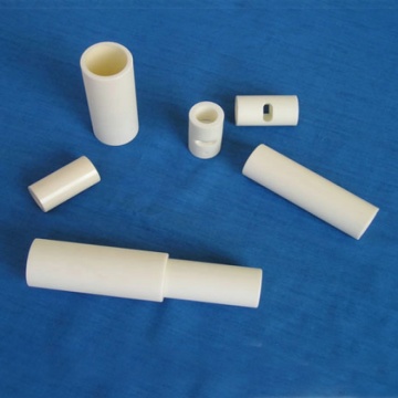
Given the properities of good heat transfer properties, vacuum tightness and minimum electric resistance, alumina Metallized ceramics are an ideal components for high vacuum ,high voltage and high pressure applications.
By applying a thin metallic coating(general Mo/Mn), by then following covered with plating, like Nickel/Copper/Gold...to the surface of the ceramic,, the welding between ceramic and metal can be achieved, which is also known as Ceramic metallization. Since tungsten and moly-Manganese metallizations have higher adhesion to the substrate than Thick-film metallization, sometimes, it's a prferred option.
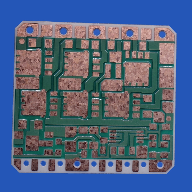
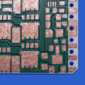
DBC (Direct bonded copper) , has excellent electrical insulation, high thermal conductivity, good solderability and high strength.It's widely used for connecting high-power semiconductor electronic circuits.
Typical application:
High-Density Hybrid Circuits, Microwave Power Devices, Power Semiconductor Devices, Power Electronic Devices, Optoelectronic Components,
Semiconductor Refrigeration Products

Q1. Is it available to provide customize products?
A: We always support custom-made metalized ceramic substrate as per different dimensions, design and metallization and plating.
Q2. When can I get the price?
A: We regularly quote within 24 hours after we get your inquiry. If you are in urgent need of getting the price, please call us or tell us in your email so that we will proceed with your inquiry as a priority.
Q3. How long can I expect to get the sample?
A: After you pay the sample charge and send us confirmed files, the samples will be ready for delivery in 4 weeks. The samples will be sent to you via express and arrive in 3-5 workdays. You can use your own express account or prepay us if you do not have an account.
Q4. How long does the whole procedure being worked out?
A: After you place an order, the manufacturing time is about 25 working days.
Q5. How to ensure quality?
A: The dimension out of any batch will be carried out sampling inspection per International AQL standard. A 100% cosmetic inspection will be done.
Q6. Are you a factory or trading company?
A: We are a professional manufacturer. We are warmly welcome clients from worldwide to visit our factory and cooperate with us.